Link to general information.
https://wiki.sipeed.com/hardware/en/tang/tang-primer-20k/primer-20k.html
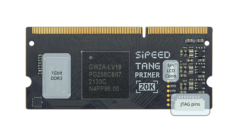
Hardware information#
User guide#
Install IDE → Learn coding programmer → Read Tutorial → Program by yourself → Read more official documents
- Install IDE: Click me.
- Visit Start to use to avoid some problems, and we can start coding for FPGA there.
- After coding for FPGA, if you think it difficult, here we collect some useful learning resource.
- Online FPGA tutorial: Verilog
- Online Verilog exercise:HDLBitsIf you have trouble using IDE, we have packed all documents about IDE, visit Download station and download what you need.
Reference examples summary#
1. Examples#
github :GitHub - sipeed/TangPrimer-20K-example: TangPrimer-20K-example project
2. Tutorial#
Additional message#
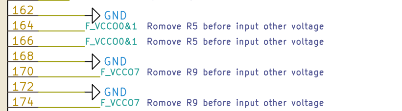
The default bank voltage of bank 0、bank 1、bank 7 on the core board is 3.3V, so their bank IO voltage is 3.3V output. If you want to custom the input IO bank voltage, please remove R5 and R9, see Assembly Click me to see where is R5 and R9.
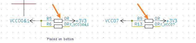
And the corresponding golden finger on core board are as following:
9. Questions#
9.1. Dock ext-board not work#
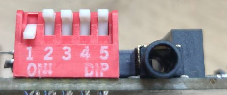
For 20K Dock kits, it’s necessary to enable the core board before using debugger debug the chip, just put the 1 switch on the dip switch down, otherwise LED0 and LED1 are on and core board dose not work.
| Enable Core Board | Disable state | Additional comments |
|---|---|---|
 |
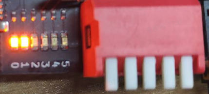 |
When disabled, the LDE0 and LED1 is on, and core board doesn’t work. |
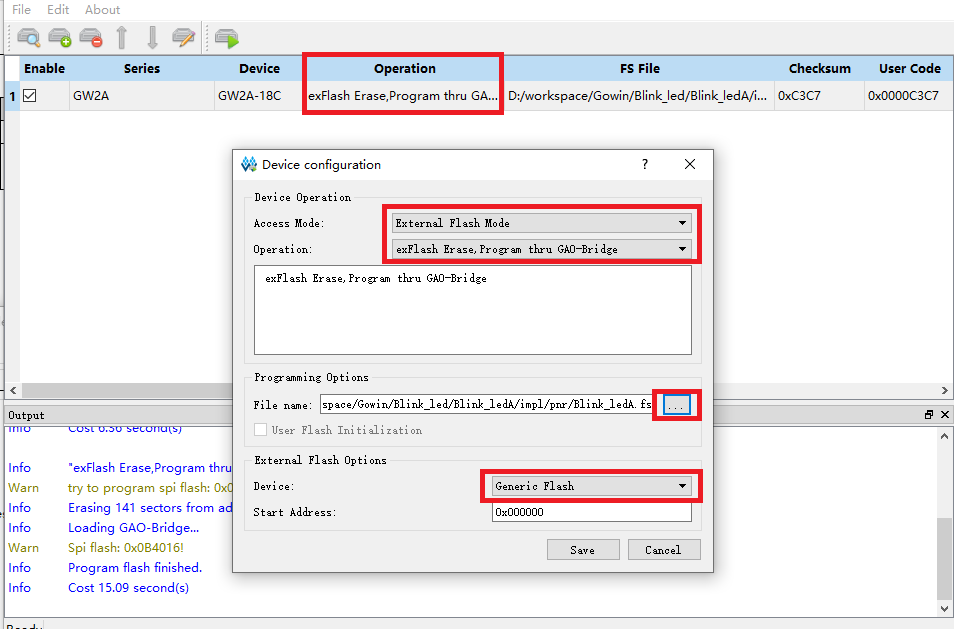
9.2. How to burn into flash#
Do following configurations:
9.3. No reaction after burning or phenomenon is wrong#
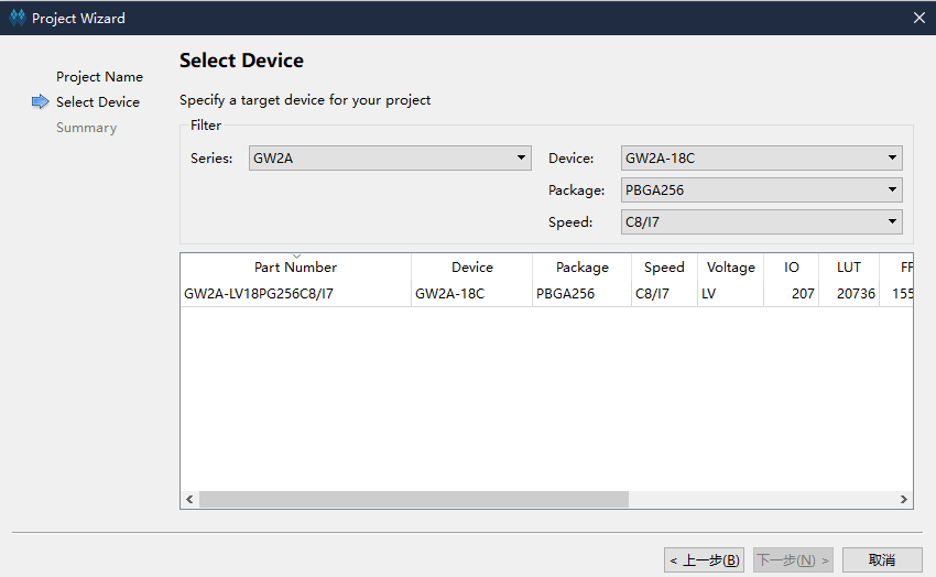
Make sure you hace selected right device, and all parameters are the same as following.
Then make sure your code logic is right and your
9.4. Successfully burned once, but can’t burn after that#
Note that the description is there was a successful Flash burnt one time.
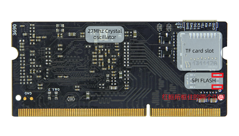
In this case, the default reason is that the wrong Dual-Purpose pin is enabled and the debugger can no longer scan the FPGA’s JTAG. You can short pin 1 and pin 4 of Flash, by which the chip cannot read FLASH normally when it is powered on.
Besides, if you have dock ext-board, this can be solved by the enable pin of dip switch. Here art the steps
Firstlt, enable the core board, put the 1 switch on the dip switch down, then do something (like burnning fpga or erasing FPGA) in Programmer application, when the progress bar shows, switch the 1 switch on the dip switch up and down, after which you will find the progress bar works and finish your operations on fpga.